Research Spotlight: Featured Article – Wonder Materials at the Pencil Tip
By Xiao-Xiao Zhang
What does the world look like when things become two-dimensional (2D), or flattened down? Two-dimensional (2D) materials have been attracting intense attention for decades. While the physical laws remain the same as in 3D, particle movements are restricted to two dimensions and electromagnetic fields can be bent, leading to completely different physical phenomena that cannot be achieved in the three-dimensional (3D) world. Physicists and engineers are intrigued because 2D materials offer a pathway to building devices that take minimal vertical space, as well as nanoscale transistors and sensors.
Ever since the isolation of graphene — a single atomic layer of carbon atoms from graphite —was awarded the 2010 Nobel Prize in Physics, the field of 2D materials, specifically the so-called van der Waals materials, has boomed. In 2D materials, the in-plane bonds are covalent (strong), while the out-of-plane bonds are van der Waals (weak). This feature allows the isolation of single atomic layers of 2D crystals. Representative 2D materials include graphene and molybdenum disulfide (MoS2), both of which can serve as pencil leads and powder lubricants because of the weak friction between the crystalline planes. Through a sophisticated procedure of crystal cleavage, a monolayer of such a crystal, often with sub-nanometer thickness, can be deposited onto various substrates for further nanofabrication, manipulation, and characterization. Depending on the material composition, many different types of solid-state systems are possible, e.g., metals, semiconductors, insulators, superconductors, magnets, and topological materials, but in a 2D crystal form. These 2D materials can be further stacked on top of each other with designated alignment to form new homo- or heterostructures, providing flexible and precise approaches to material design and tuning of physical interactions, which are hard to achieve otherwise.
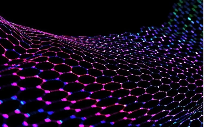
Image Credit: Marco de Benedictis/Shutterstock.com
Our laboratory has recently received two grant awards, the National Science Foundation (NSF) Early Career Award and the Department of Energy (DOE) Early Career Award, to support our optical investigations of 2D semiconductors and 2D magnets using ultrafast lasers. In the 2D semiconductor project sponsored by NSF, we study how correlated electron and hole pairs (excitons) absorb light. Understanding the intra- and inter-excitonic interactions is crucial for designing quantum devices with contact-free, all-optical control and sensing. The Coulomb attraction between electrons and holes confined to a 2D layer acts almost as if they were in a vacuum. As a result, exceptionally tightly bound excitons and multiexciton complexes have been observed in 2D crystals. Our group focuses on a special type of optically “dark” excitons in 2D semiconductors, which do not directly couple to light and thus can be accumulated to a high density, so that excitons start to overlap. The grant award will allow us to study the nonlinear interactions and quantum correlations formed within these excitons and search for potential macroscopic ordering of the exciton spin degree of freedom at low temperatures.
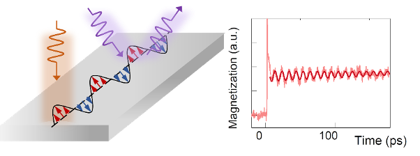
The right shows the measured spin wave oscillations in a 1.5 nanometer thick CrI3 device with micrometer lateral sizes.
Our DOE-funded research focuses on light-induced spin manipulation in 2D magnets. Magnetic crystals like CrI3 have recently been found to maintain robust ferromagnetic ordering in the monolayer limit, opening up new possibilities for the next generation of nanoscale spintronics. Here electron spin transport, instead of typical charge current transport, is used for information processing. In our lab, we use ultrafast laser pulses to trigger spin wave excitations in 2D magnets and to modify the magnetic interactions on the sub-picosecond scale (< 10-12 second). Studying how the magnetization responds to an intense laser pulse can shed light on the intrinsic spin-spin interactions and their coupling to lattice vibrations in this novel class of materials.
A lot more is happening in this field. New 2D materials can also be used as a platform for probing fundamental hypotheses, not only in condensed matter and atomic physics but even in high-energy physics, while also finding practical applications in chemistry, biology, and electrical engineering. A whole new world of science and engineering opens when we flatten things down.
Return to the Spring 2023 newsletter.